V2 Build and installation guide: Difference between revisions
No edit summary |
No edit summary |
||
| Line 1: | Line 1: | ||
*'''1. Build power supply''' | |||
*Install D2, D3, D4, D5, C1, C2 and U3. install the molex connector (X2) | **Install D2, D3, D4, D5, C1, C2 and U3. install the molex connector (X2) | ||
*Install the 3 jumpers: R12 (zero ohm resistor), J1 and the "unlabeled" jumper that is just to the left of the processor. | **Install the 3 jumpers: R12 (zero ohm resistor), J1 and the "unlabeled" jumper that is just to the left of the processor. | ||
<center> | <center> | ||
| Line 17: | Line 17: | ||
'''Ensure proper power supply polarity or you may damage the 6 programmable output transistors.''' | '''Ensure proper power supply polarity or you may damage the 6 programmable output transistors.''' | ||
*Test for proper +5v and ground on the following components: | **Test for proper +5v and ground on the following components: | ||
*Processor (Pin 1 GND, Pin 16 +5v) | **Processor (Pin 1 GND, Pin 16 +5v) | ||
*MAX 232 (Pin 15 GND, Pin 16 +5v) | **MAX 232 (Pin 15 GND, Pin 16 +5v) | ||
*Oscillator (pins are numbered strangely, but GND is the lower right pin and +5v is the upper left, when viewing from the component side) | **Oscillator (pins are numbered strangely, but GND is the lower right pin and +5v is the upper left, when viewing from the component side) | ||
*MAP sensor ( pin 2 is GND, pin 3 is +5v. "dot" is next to pin 1 on solder side) | **MAP sensor ( pin 2 is GND, pin 3 is +5v. "dot" is next to pin 1 on solder side) | ||
| Line 29: | Line 29: | ||
#'''Install remaining components''' | #'''Install remaining components''' | ||
*Insert all of remaining resistors, capacitors, diodes and transistors, <b>except for the oscillator (QG1) and MAP sensor</b> ** make sure you use the right zener diodes in the correct places! | **Insert all of remaining resistors, capacitors, diodes and transistors, <b>except for the oscillator (QG1) and MAP sensor</b> ** make sure you use the right zener diodes in the correct places! | ||
(insert reference picture for transistor alignment) | (insert reference picture for transistor alignment) | ||
*Install the IC sockets and the DB9 connector | **Install the IC sockets and the DB9 connector | ||
<center> | <center> | ||
| Line 39: | Line 39: | ||
</center> | </center> | ||
*Power up the circuit and repeat the power supply steps outlined in step 1. '''This is critical to prevent damage to the integrated circuits due to circuit faults.''' | **Power up the circuit and repeat the power supply steps outlined in step 1. '''This is critical to prevent damage to the integrated circuits due to circuit faults.''' | ||
#'''3. Final assembly''' | #'''3. Final assembly''' | ||
| Line 45: | Line 45: | ||
*Solder the oscillator. Note the orientation of the oscillator- the sharp corner of the oscillator can matches the silkscreen on the board. | *Solder the oscillator. Note the orientation of the oscillator- the sharp corner of the oscillator can matches the silkscreen on the board. | ||
*Solder in the Map sensor. the map sensor fits "upside down" with the vent pointing down. Also- the sensor's pin #1 is aligned with the the "dot" on the solder side of the board. The MAP sensor's pin #1 has a notch in it. | **Solder in the Map sensor. the map sensor fits "upside down" with the vent pointing down. Also- the sensor's pin #1 is aligned with the the "dot" on the solder side of the board. The MAP sensor's pin #1 has a notch in it. | ||
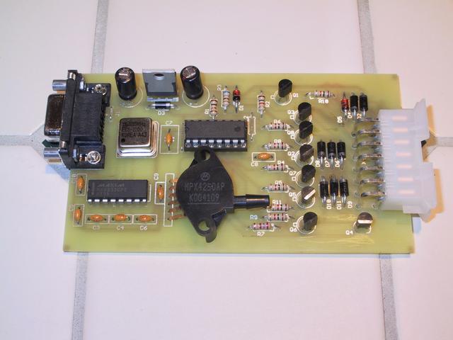
*Plug in the processor and MAX 232. Note the orientation of the processors- the notch of the processor aligns with the notch in the silkscreen. | **Plug in the processor and MAX 232. Note the orientation of the processors- the notch of the processor aligns with the notch in the silkscreen. | ||
<center> | <center> | ||
Revision as of 00:35, 4 February 2007
- 1. Build power supply
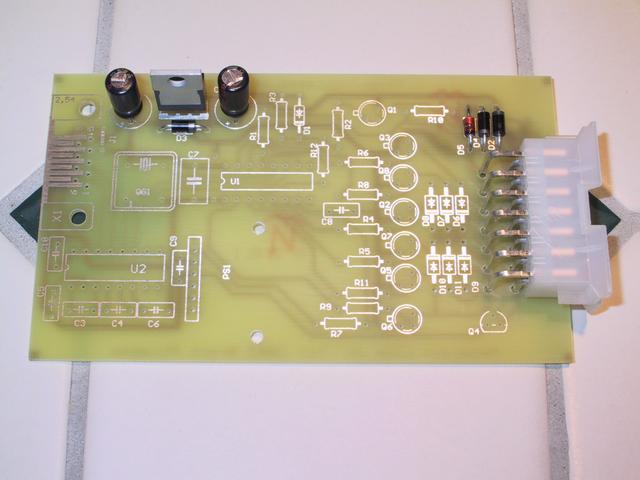
- Install D2, D3, D4, D5, C1, C2 and U3. install the molex connector (X2)
- Install the 3 jumpers: R12 (zero ohm resistor), J1 and the "unlabeled" jumper that is just to the left of the processor.
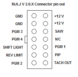
Power up the unit. Refer to the following diagram on the molex connector:
Ensure proper power supply polarity or you may damage the 6 programmable output transistors.
- Test for proper +5v and ground on the following components:
- Processor (Pin 1 GND, Pin 16 +5v)
- MAX 232 (Pin 15 GND, Pin 16 +5v)
- Oscillator (pins are numbered strangely, but GND is the lower right pin and +5v is the upper left, when viewing from the component side)
- MAP sensor ( pin 2 is GND, pin 3 is +5v. "dot" is next to pin 1 on solder side)
Do not proceed to the next step until proper power supply operation is verified.
- Install remaining components
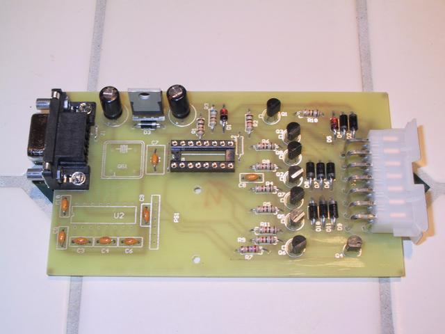
- Insert all of remaining resistors, capacitors, diodes and transistors, except for the oscillator (QG1) and MAP sensor ** make sure you use the right zener diodes in the correct places!
(insert reference picture for transistor alignment)
- Install the IC sockets and the DB9 connector
- Power up the circuit and repeat the power supply steps outlined in step 1. This is critical to prevent damage to the integrated circuits due to circuit faults.
- 3. Final assembly
- Solder the oscillator. Note the orientation of the oscillator- the sharp corner of the oscillator can matches the silkscreen on the board.
- Solder in the Map sensor. the map sensor fits "upside down" with the vent pointing down. Also- the sensor's pin #1 is aligned with the the "dot" on the solder side of the board. The MAP sensor's pin #1 has a notch in it.
- Plug in the processor and MAX 232. Note the orientation of the processors- the notch of the processor aligns with the notch in the silkscreen.

Remaining components installed
Power up and test voltages again- no smoke is a good sign. :)


